EpiPhotonics pioneers and leads the design and manufacture of PLZT thin-film
waveguide technology. PLZT is one of most attractive materials for the
integration of high-channel count and/or various photonic functions into
a small monolithic chip, with high-speed control and low-power dissipation.
Its efficient, voltage-induced index change, that is, the electro-optic
effect, enable thermal cross-talk free integration, miniaturization of
electrodes, and low power dissipation. Moreover, its suitable high refractive
index (2.45) decreases the bending radius of a classic waveguide.
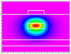
PLZT optical switches have a MMI-MZ (Multi Mode Interference-Mach Zhender)
type switch design with wavelenth insensitive nature. The PLZT growth and
the PLZT waveguide are described below.

EpiPhotonics succeeded in producing the world's
first low-loss, thin-film waveguide
by using
solid-phase epitaxy (SPE). SPE
differs from
widely used vapor-phase growth
technologies,
such as sputtering and MOCVD.
In our process,
uniquely synthesized metal organic
solutions
are applied to substrates and
heated at ambient
pressure to form amorphous films.
These films
are then heated to create epitaxial
single-crystals.
This manufacturing SPE method
is extremely
simple and eliminates the need
for large-scale
vacuum equipment, making it possible
for
drastic cost reduction.
 Buried PLZT waveguides are grown on Nb:SrTiO3 semiconductor substrates in order to facilitate application of electrical field. Using this sandwiched electrode structure and combining it with PLZT's inherently high electro-optic coefficient, we have achieved drastic improvements in switching and/or modulating performances;
- High-speed switching (<5ns)
- Low driving voltage
- Low insertion loss
- Low polarization dependence
- Low power consumption
- Miniaturization
Solid-phase epitaxial growth technology combined with our micro-fabrication
technique, guarantees huge cost reduction. Exploiting the high index nature
of our material and realizing a buried waveguide, low-loss sharp S-bends
and efficient waveguide structure are assured. This allows us to produce
very compact waveguide devices including switches, modulators, and AWGs
At EpiPhotonics, we excel in creating innovative and efficient products
based on our proprietary thin film PLZT waveguide technology based on design
and manufacturing processes refined over decades of research and development.
The devices utilizing the technology enabled us to develop high-speed integrated
subsystems with performance levels that were deemed impossible a short
time ago. EpiPhotonics's success and ability to compete depends on its
ability to develop technological expertise internally. EpiPhotonics relies
on a combination of patent and trade secret laws. EpiPhotonics' intellectual
property is protected by a portfolio of more than 50 patents, including
transferred patents from Keio University, in the United States and in Japan.
The patents portfolio covers precursor synthesis,
thin-film growth, micro-fabrication, waveguide
structure, integration on semiconductor,
and device structures.
 | Nano-Second Speed PLZT Waveguide Switches
and Filters |